QRM#
Description#
The Qubit Readout Module (QRM) is an instrument designed for performing qubit readout. The front of a QRM module is presented below:
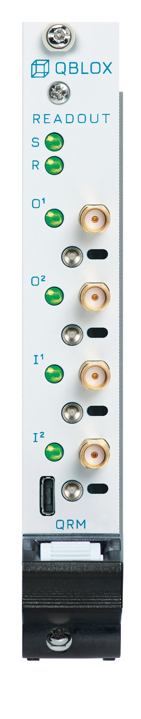
On the front of a QRM module you will find the following components:
4 x SMA female (receptacle) connectors: 2 outputs (O[1-2]: 1 Vpp @ 50 Ω) ; and 2 input channels (I[1-2]: 2 Vpp @ 50 Ω).
4 x SMP male (pin) connectors: Marker output channels (0-3.3 V TTL).
6 x status LEDs: See section Frontpanel LEDs for details.
These input paths use two processing paths (from here on also referred to as path 0 and 1). The module has 6 Q1 sequencers (Q1 Sequence Processor) on board with the following architecture:

Each sequencer is connected to each marker and each sequencer can access the outputs and inputs of the device across their respective paths. In the case of the QRM, each sequence processor has control over one AWG and one acquisition path.
Using parametrization, each sequencer can target one qubit for readout, allowing multiplexed readout of multiple qubits on the same channel. The AWG can generate the readout pulses and the acquisition paths can process the returned readout data. The acquisition path supports three acquisition modes:
Scope: Returns the raw input data.
- Integration: Returns the result after integrating the input data;
optionally based on an integration function stored in memory.
- Thresholded: Returns the binary qubit value after thresholding
the integrated value.
The results of the acquisitions are returned to the user through the qblox_instruments driver.
For a list of available features please go to Features
For an overview of applications please go to Applications
Block Diagram#

Features#
1. 10 MHz Reference#
Alongside all modules available, the QRM baseband module operates with respect to a 10 MHz reference provided by the cluster.
2. Trigger#
The trigger of the QRM is connected to the cluster and allows for fast synchronization between modules.
3. SYNQ#
The Qblox SYNQ technology enables simple and quick synchronization over multiple instruments, allowing for modules to be started synchronously << 1ns. See section Synchronization for more information.
4. LINQ#
The Qblox LINQ technology allows for the results of measurements to be shared between devices, distributing outcomes in < 320 ns.
5. Q1 Sequencers#
The Q1 sequencers are the heart(s) of the QRM instrument. They orchestrate the experiment using a custom low-latency sequence processor specifically designed for quantum experiments. Each sequencer controls a dedicated AWG path and, in the case of a QRM/QRM-RF, an acquisition path, which enables parametrized pulse generation and readout. Each QRM has 6 of these sequencers to target multiple qubits with one instrument. See section Q1 Sequence Processor for more information on how to program and control them, as well as a list of available features that each sequencer provides.
Each sequencer has a dedicated gain step for both path 0 and 1, which can be
statically configured using the Sequencer.gain_awg_path0() parameters.
However, the gain can also be dynamically controlled using the set_awg_gain
instruction of the sequence processor which enables pulse parametrization
(see section Instructions). The static and
dynamic gain controls are complementary.
Note
If modulated IQ signals are used for an output pair, the gain
Sequencer.gain_awg_path0() has to be the same for both paths.
Each sequencer has a dedicated numerically controlled oscillator (NCO). This NCO can be used to track the qubit phase (at a fixed frequency). This NCO can be swept from -500 MHz to 500 MHz
The frequency of the NCO and phase can be statically controlled using the
Sequencer.nco_freq() and Sequencer.nco_phase_offs()
parameters. However, the phase of the NCO can also be dynamically controlled
using the set_freq, reset_ph, set_ph, and set_ph_delta instructions of
the sequence processor, which enables
pulse parametrization and execution of virtual Z-gates
(see section Instructions). The static and
dynamic phase control
is complementary. The modulation is enabled using the
Sequencer.mod_en_awg() parameter. The demodulation is enabled using
the Sequencer.demod_en_acq() parameter.
Each sequencer can perform averaging and binning of measurement of results. Integration and state assignment of data can also be performed on board, outcomes of these measurements can then be shared via LINQ within 200ns.
6. Marker output channels#
Each sequencer has control over the four marker output channels, with the
control of each sequencer being OR’ed to create the final marker outputs.
The markers can
be dynamically controlled with the set_mrk instruction of the sequence
processor (see section Instructions), but can
also, be overwritten with the static marker overwrite parameters
Sequencer.marker_ovr_en() and Sequencer.marker_ovr_value().
The marker output range is 0-3.3 V TTL. In RF modules set_mrk
is also used to toggle the switches before the outputs/inputs to enable
the respective output/input.
6.1 Setting Markers as Active HIGH/LOW#
The default state of marker is active high (OFF = 0 V, ON = 3.3 V). Users
have the ability to change the marker output from active HIGH to active LOW ( OFF = 3.3 V, ON = 0 V). It can be done
using the parameter QRM.marker0_inv_en(). This inversion of marker default states is possible for all marker
channels.
7. Sequencer Multiplexer#
A multiplexer that allows any sequencer to be connected to any output. Multiple sequencers can also be connected to a single output. This, in combination with the dedicated NCO per sequencer and an external IQ mixing circuit, enables easy and flexible targeting of multiple resonators on a single channel. See Multiplexing for more details.
Note
The output of each sequencer is complimentary. Be aware of potential output clipping when connecting multiple sequencers to a single output.
8. Digital Offset#
Each sequencer has a dedicated offset step for both path 0 and 1, which can be
statically configured using the Sequencer.offset_awg_path0() parameters.
However, the offset can also be dynamically controlled using the set_awg_offs
instruction of the sequence processor which enables pulse parametrization.
(see section Instructions). The static and dynamic
offset controls are complementary.
Note
This offset is applied to the signals before the mixer and cannot be used for DC offset correction if the mixer is enabled.
9. DAC#
The maximum output and input range of the QRM is 1 Vpp and it is 50 Ω terminated.
10. ADC#
The maximum input range of the QRM’s ADCs is 2 Vpp and 50 Ω terminated.
Note
The 12-bit ADCs have a fixed range of 2 Vpp. When performing acquisitions the input should be an order of magnitude such that the resolution (0.5mV) of the ADC can accurately define the measured signal. Gain or attenuation stages may be required at the input to compensate for this.
11. Input gain#
Dedicated amplifiers provide additional gain to the input signals. The gain
can vary between -6 dB and 26 dB and can be set using the QRM.in0_gain()
parameters.
Applications#
The qubit readout module (QRM) is designed for the measurement of qubits. The experimental setup will vary depending on the device being measured:
Superconducting Qubits#
The QRM can be utilized to create a readout pulse with its outputs and corresponding acquisition for a multi qubit device. Frequency division multiplexing can be utilized to readout multiple qubit states simultaneously. The outputs of a QRM can also be utilized as arbitrary outputs (e.g. for a charge line) if needed. The baseband of the QRM module will not be able to synthesize frequencies in the range required for readout, and as such a QRM-RF module or, alternatively, an external rf conversion circuit will be required. The details of such a setup are provided here: Superconducting Qubits.
Spin Qubits#
The QRM provides readout utility for measuring spin qubits in GaAs, Si or Ge quantum dots. The QRM is capable of performing qubit measurements via charge sensing, RF reflectometry, gate-based readout, or microwave resonators. The signal of the baseband QRM module should be upconverted using an external rf conversion circuit to reach the microwave readout regime. Alternatively, a QRM-RF module can be used. Details of potential setups and applications are available here: Spin Qubits.
NV-centers/Spins in Diamonds#
The QRM can also be used to perform measurements on spins in diamond by acquiring analog and digital signals from single photon detectors and perform trigger counting on these signals to determine the number of emitted photons. These results can be shared using the LINQ protocol and thresholded for conditional operation on any other module in the cluster. Additionally, the QRM can also perform measurements through the connection to a qubit’s microwave resonator. The signal of the baseband QRM module should be upconverted using an external rf conversion circuit to reach the microwave readout regime. Alternatively, a QRM-RF module can be used. Details of potential setups and applications are available here : NV-centers.
Absolute Maximum Ratings#
Warning
This section shows the absolute maximum ratings of the cluster QRM module. Operation beyond these values can damage the module and cluster!
Parameter |
Condition |
Min |
Typ |
Max |
|---|---|---|---|---|
Voltage applied to output |
-5V |
+5V |
||
Voltage applied to input |
-2.5V |
+2.5V |
||
Marker load impedance |
66Ω |
Specifications#
Output#
Parameter |
Condition |
Min |
Typ |
Max |
|---|---|---|---|---|
Number of channels |
2 |
|||
Output coupling |
DC |
|||
Resolution |
12bits |
|||
Output impedance |
50Ω |
|||
Output range |
In 50Ω load |
+-0.5V |
Input#
Parameter |
Condition |
Min |
Typ |
Max |
|---|---|---|---|---|
Number of channels |
2 |
|||
Input coupling |
DC |
|||
Resolution |
12bits |
|||
Input impedance |
50Ω |
|||
Input range |
settable amplification |
+-0.025V |
+-1V |
Marker Outputs#
Parameter |
Condition |
Min |
Typ |
Max |
|---|---|---|---|---|
Number of markers |
4 |
|||
High voltage |
in high Z load |
3.3V |
||
Low voltage |
0.0V |
Typical Performance#
Output#
Parameter |
Value |
Test specifics |
|---|---|---|
Voltage range |
+-0.5 V |
Measured with a 1MHz block wave in 50Ω load |
Rise/Fall time |
<1.3 ns |
Measured with a 1V step in 50Ω load, 10% - 90% |
Settling time |
<8 ns |
Measured with a 1V step in 50Ω load, settled within +-1% |
Overshoot |
<1% |
Measured with a 1V step in 50Ω load |
Crosstalk step |
<-75 dB |
Measured with a 1V step in 50Ω load |
Crosstalk sine |
<-70 dB |
Measured with a 100MHz 1Vpp sine wave in 50Ω load |
Frequency response |
>300 MHz |
Bandwidth (-4dB) |
Frequency response |
>400 MHz |
Bandwidth (-7dB) |
Wideband noise |
<5 nV/sqrtHz |
Noise measured at 121Mhz with 1kHz band and 0V output |
Output RMS noise |
<70 uVrms |
Based on bandwidth and wideband noise |
Signal to noise ratio |
>87 dB |
Based on the output RSM voltage O8 |
Total harmonic distortion |
THD <0.0012 |
Measured at 100MHz sine wave up to the fifth harmonic |
HD2 |
HD2 <-59 dBc |
Measured at 100MHz sine wave up to the fifth harmonic |
HD3 |
HD3 <-60 dBc |
Measured at 100MHz sine wave up to the fifth harmonic |
Input#
Parameter |
Value |
Test specifics |
|---|---|---|
Voltage range |
+-1 V |
|
Rise/Fall time |
1.5 ns |
10% to 90% |
Overshoot rise |
1.8% |
|
Overshoot fall |
4% |
|
Settling time |
30 ns |
Settled within +-1% |
Input-input crosstalk |
<-90 dB |
|
Frequency response |
>350 MHz |
Bandwidth (-3dB) |
Frequency response |
>450 MHz |
Bandwidth (-5dB) |
Low frequency noise at -6 dB gain |
500 uVpp |
0.1-10 Hz integrated |
Low frequency noise at 26 dB gain |
<20 uVpp |
0.1-10 Hz integrated |
Harmonic distortion HD2 |
<= -63 dBc |
~1 dBm input |
Harmonic distortion HD3 |
<= -65 dBc |
~1 dBm input |
SNR -6 dB gain |
~60 dB |
|
SNR 26 dB gain |
~50 dB |
|
Wideband noise at -6 dB gain |
< 43 nV/sqrtHz |
At 100 MHz |
Wideband noise at 26 dB gain |
< 4 nV/sqrtHz |
At 100 MHz |
Wideband noise at -6 dB gain |
<700 uVrms |
integrated over 300 MHz |
Wideband noise at 26 dB gain |
<60 uVrms |
integrated over 300 MHz |