QCM#
Description#
The Qubit Control Module (QCM) is an instrument completely dedicated to qubit control using parametrized pulses. The front of a QCM module is presented below:
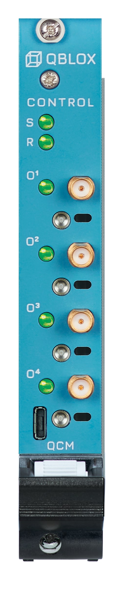
On the front of a QCM module you will find the following components:
4 x SMA female (receptacle) connectors: 4 outputs (O[1-4] @ 50 Ω).
4 x SMP male (pin) connectors: Marker output channels (0-3.3 V TTL).
6 x status LEDs: See section Frontpanel LEDs for details.
The pulses are stored as waveform envelopes in memory and can be parametrized by changing gain and offset and additionally, phase if also modulated. This is all managed by Qblox’s Q1 sequencer processors (see here for more information Q1 Sequence Processor). The QCM has 6 of these processors on board, with the following architecture:

Parametrization of pulses is controlled by the AWG of the sequencers, which each have two waveform paths (from here on referred to as path 0 and 1). Using parametrization, the output of these paths can either be independent signals or modulated IQ signals. The two paths of each sequencer can, in turn, be connected to any output pair of the instrument (i.e. O1/2 or O3/4) to control one or more qubits per output. Additionally, each sequencer can control the four marker output channels.
For a list of available features please go to Features
For an overview of applications please go to Applications
Block Diagram#

Features#
1. 10MHz Reference#
Alongside all modules available, the QCM baseband module operates with respect to a 10MHz reference provided by the cluster.
2. Trigger#
The trigger of the QCM is connected to the cluster and allows for fast synchronization between modules.
3. SYNQ#
The Qblox SYNQ technology enables simple and quick synchronization over multiple instruments, allowing for modules to be started synchronously << 1ns. See section Synchronization for more information.
4. LINQ#
The Qblox LINQ technology allows for the results of measurements to be shared between devices, distributing outcomes in < 320ns.
5. Q1 Sequencers#
The Q1 sequencers are the heart(s) of the QCM instrument. They orchestrate the experiment using a custom low-latency sequence processor specifically designed for quantum experiments. Furthermore, they each achieve that by controlling a dedicated AWG path and, in the case of a QCM/QCM-RF, an acquisition path, which enables parametrized pulse generation and readout. Each instrument has 6 of these sequencers to target multiple qubits with one instrument. See section Q1 Sequence Processor for more information on how to program and control them.
Each Q1 sequencer has a dedicated numerically controlled oscillator (NCO). This NCO can be used to track the qubit phase (at a fixed frequency) in real-time. This NCO can be swept from -500MHz to 500MHz.
The frequency of the NCO and phase can be statically controlled using the
Sequencer.nco_freq() and Sequencer.nco_phase_offs()
parameters. However, the frequency and phase of the NCO can also be dynamically controlled
using the set_freq, reset_ph, set_ph and set_ph_delta instructions of
the sequence processor, which enables
pulse parametrization and execution of virtual Z-gates
(see section Instructions). The static and dynamic phase
control is complementary. The modulation is enabled using the
Sequencer.mod_en_awg() parameter. The demodulation is enabled using the
Sequencer.demod_en_acq() parameter.
Each sequencer has a dedicated gain step for both path 0 and 1, which can be
statically configured using the Sequencer.gain_awg_path0() parameters.
However, the gain can also be dynamically controlled using the set_awg_gain
instruction of the sequence processor which enables pulse parametrization
(see section Instructions). The static and dynamic
gain controls are complementary.
Note
If modulated IQ signals are used for an output pair, the gain
Sequencer.gain_awg_path0() has to be the same for both paths.
6. Marker Output Channels#
Each sequencer has control over the four marker output channels, with the
control of each sequencer being OR’ed to create the final marker outputs.
The markers can be dynamically controlled with the set_mrk instruction of the
sequence processor (see section Instructions), but can
also be overwritten with the static marker overwrite parameters
Sequencer.marker_ovr_en() and Sequencer.marker_ovr_value().
The marker output range is 0-3.3 V TTL. In RF modules set_mrk is also used to
toggle the switches before the outputs/inputs to enable the respective
output/input.
6.1 Setting Markers as Active HIGH/LOW#
The default state of marker is active high (OFF = 0V, ON = 3.3V). Users
have the ability to change the marker output from active HIGH to active LOW ( OFF = 3.3 V, ON = 0V). It can be done
using the parameter QCM.marker0_inv_en(). This inversion of marker default states is possible for all marker
channels.
7. Sequencer Multiplexer#
A multiplexer that allows any sequencer to be connected to any output. Multiple sequencers can also be connected to a single output. This, in combination with the dedicated NCO per sequencer and an external IQ mixer circuit, enables easy and flexible targeting of multiple qubits on a single channel. See Multiplexing for more details.
Note
The output of each sequencer is complimentary. Be aware of potential output clipping when connecting multiple sequencers to a single output.
8. Digital Offset#
Each sequencer has a dedicated offset step for both path 0 and 1, which can be
statically configured using the Sequencer.offset_awg_path0() parameters.
However, the offset can also be dynamically controlled using the set_awg_offs
instruction of the sequence processor which enables pulse parametrization.
(see section Instructions). The static and dynamic offset
controls are complementary.
Note
This offset is applied to the signals before the mixer and cannot be used for DC offset correction if the mixer is enabled.
9. DAC#
The dynamic output range of the QCM’s DACs is 5 Vpp and 50 Ω terminated at 1GBps.
10. Offset DAC#
The offset DAC allows users to apply a DC offset to the output signal without the risk of clipping the signal at the DAC.
Applications#
The Qubit control module (QCM) is designed to be utilized for the control of qubits. The experimental setup will vary depending on the device being controlled:
Superconducting Qubits#
The QCM can be utilized to generate superconducting qubit drive frequencies or to generate signals to tune qubit transition frequencies. QCM modules can be utilized to drive SQUID loops both with and without an extra DC source. An external RF mixing circuit (e.g. IQ mixer etc.) will be required to convert signals in the baseband of the QCM (0-400MHz) to the desired drive signal. The details of such a setup are provided here: Superconducting Qubits.
Spin Qubits#
The QCM module can be used to generate control signals for GaAs, Si and Ge spin qubits. To do this an external RF mixing circuit will be required to convert from the QCM baseband (0-400MHz) to the qubit frequency. SPI DC sources can be coupled with QCM baseband modules via bias tees and connected to gates for tuning barrier potentials and fast gate sweeps. Details of potential setups and applications are available here: Spin Qubits.
NV-centers/Spins in Diamonds#
The QCM module can be used to generate control pulses for spins in diamond. An external RF mixing circuit will be required to convert from the QCM baseband (0-400MHz) to the desired qubit frequency. Details of potential setups and applications are available here : NV-centers.
Absolute Maximum Ratings#
Warning
This section shows the absolute maximum ratings of the cluster QCM module. Operation beyond these values can damage the module and cluster!
Parameter |
Condition |
Min |
Typ |
Max |
|---|---|---|---|---|
Voltage applied to output |
-5V |
+5V |
||
Marker load impedance |
66Ω |
Specifications#
Outputs#
Parameter |
Condition |
Min |
Typ |
Max |
|---|---|---|---|---|
Number of channels |
4 |
|||
Output coupling |
DC |
|||
Resolution |
16bits |
|||
Output impedance |
50Ω |
|||
Output range |
In 50Ω load |
+-2.5V |
||
Analog offset voltage range |
+-80mV |
Marker Outputs#
Parameter |
Condition |
Min |
Typ |
Max |
|---|---|---|---|---|
Number of markers |
4 |
|||
High voltage |
in high Z load |
3.3V |
||
Low voltage |
0.0V |
Typical Performance#
Output#
Parameter |
Value |
Test specifics |
|---|---|---|
Voltage range |
+-2.5 V |
Measured with a 1MHz block wave in 50Ω load |
Rise time |
<1.4 ns |
Measured with a 1V step in 50Ω load, 10% - 90% |
Settling time |
<8 ns |
Measured with a 1V step in 50Ω load, settled to +-1% |
Overshoot |
<1% |
Measured with a 1V step in 50Ω load |
Crosstalk step |
<-65 dB |
Measured with a 5V step in 50Ω load at 100 MHz |
Crosstalk sine |
<-70 dB |
Measured with a 5Vpp sine wave in 50Ω load at 100 MHz |
Output bandwidth |
>215 MHz |
-3dB point |
>400 MHz |
-9dB point |
|
Output RMS noise |
<100 uVrms |
Based on the bandwidth of 220 MHz at -3dB point |
Wideband noise |
<6.5 nV/sqrtHz |
Noise measured at 121Mhz with 1kHz band and 0V output |
Signal to noise ratio |
>80 dB |
Based on the output RMS noise voltage |
Total harmonic distortion (HD) |
<0.006 |
Measured at 100MHz sine wave up to the fifth harmonic, over the full output voltage swing |
HD2 |
<-45 dBc |
Measured at 100MHz sine wave up to the fifth harmonic, over the full output voltage swing |
HD3 |
<-50 dBc |
Measured at 100MHz sine wave up to the fifth harmonic, over the full output voltage swing |
Total harmonic distortion (HD) |
<0.0015 |
Measured at 100MHz sine wave up to the fifth harmonic, at 1Vpp output voltage |
HD2 |
<-65 dBc |
Measured at 100MHz sine wave up to the fifth harmonic, at 1Vpp output voltage |
HD3 |
<-60 dBc |
Measured at 100MHz sine wave up to the fifth harmonic, at 1Vpp output voltage |